Introduction
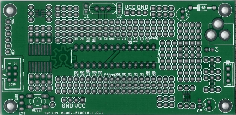
This page contains the (relatively unchanging) information about v0.1 of the SARduino328 board.

SARduino328 v0.1
Design Files
Bill of Materials
| Designator |
Value |
Purpose |
| IC2 |
ATmega328 |
Microcontroller (or ATmega8 or ATmega168) |
| R1 |
10K ohm |
Pullup resistor for RESET switch |
| Y1 |
16MHz Crystal |
Oscillator (or 16MHz Ceramic Resonator, omit C1,C2) |
| C1,C2 |
18-30pF Cap |
Capacitors for Crystal (match required value) |
| C4,C5 |
0.1uF Cap |
Bypass capacitors for MCU, consider putting right at 5V/GND and A+/GND pins instead of labeled positions |
| JP10 |
1×6 header |
6-pin FTDI cable programming connection (optional) |
| SV1 |
2×3 header |
6-pin ISP programming connection (optional), shrouded or bare |
| JP6 |
1×3 header |
3-pin power selector (external or USB) |
| External Power Supply Option: |
| D1 |
1N400X |
Input protection diode (e.g., 1N4001 or 1N4004) |
| J? |
2.1mm jack |
External Power Jack |
| VR-TOP |
7805 |
5V Regulator (any IN-GND-OUT should work, or 3V3 if you want that) |
| C6,C7 |
10uF-100uF |
Power Supply Filter Caps |
Errata
- The reference designators are all jacked up on this one.
- Most passives are not labeled by value on the PCB.
- There is no cap on the reset line from the FTDI to support auto-reset.
- Some extra power and ground rails would be nice for prototyping.
- It would also be nice to have a pad for raw external VIN, in case we’re not using a 2.1mm jack.
- C4 and C5 are really bypass caps for the microcontroller, and should be as close to the VCC pins as possible. Omit from marked placement, and instead put right across power/ground pins on each side of the microcontroller.

